
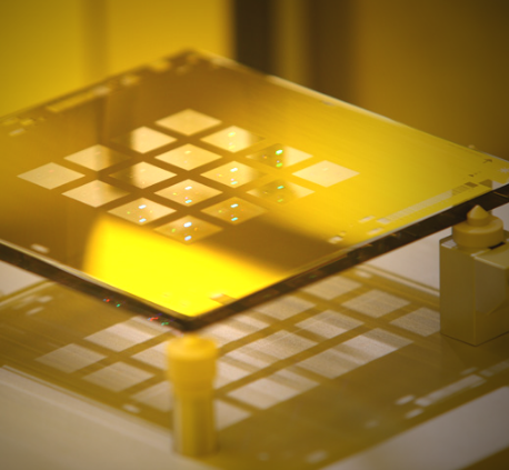
Headquartered in Brookfield, Connecticut, Photronics is a world leader in the critical photomasks used to manufacture semiconductor wafers. Photomasks are those glass or quartz plates that contain microscopic images of electronic circuits. They are unique to each customer’s design, confidential, and manufactured in layers of distinct etched patterns.
Photronics was founded in 1969 as Photronic Labs in Danbury, Connecticut, and since then has acquired photomask business units of companies including Martin Marietta, Analog Devices, Unisys, Texas Instruments, Motorola, and Conexant, among others.
Because the first several layers of photomasks often must be delivered to customers within 24 hours of receiving the design, Photronics maintains a laser focus on R&D and the efficiency of all processes. R&D takes place mostly at the firm’s facility in Boise, Idaho, and to a lesser degree, subsidiaries in Taiwan and South Korea, where future development is focused on specific customer projects as well as nanotechnology, new TV technology, emerging micro- and mini-LED displays and mobile displays. According to the firm’s most recent annual report, Photronics considers its R&D investment to be key to its ability to maintain leadership in its category. The firm’s management believes the rich stores of intellectual property accumulated over the 53 years since the firm’s founding provide an edge in the highly competitive global photomask business.
As of 6/30/22, Photronics was held in the Knowledge Leaders Strategy.

Image and article originally from www.knowledgeleaderscapital.com. Read the original article here.